Objective
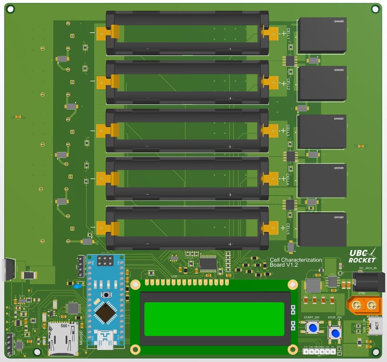
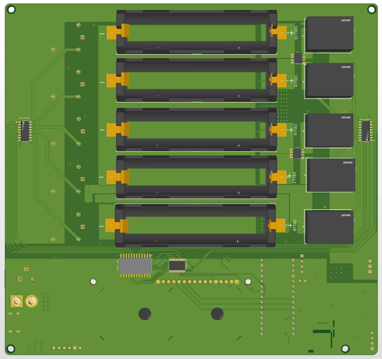
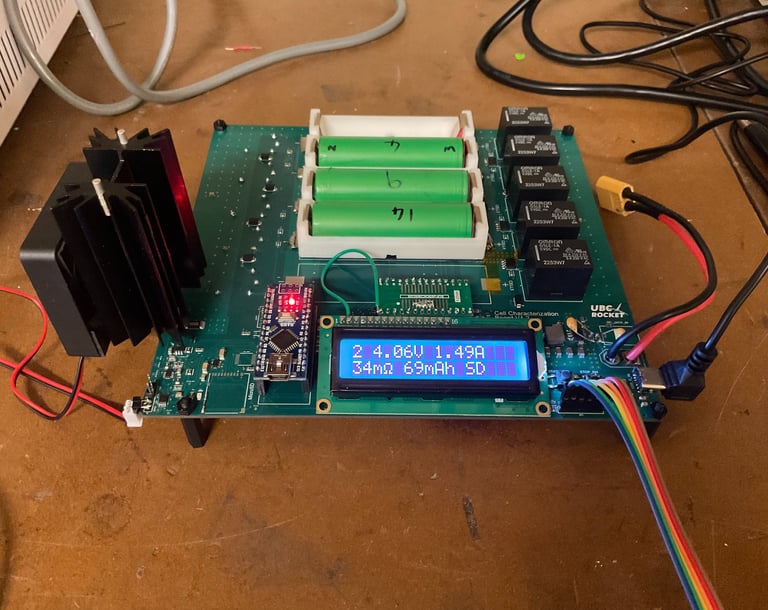
Build a 10-channel sequential lithium-ion cell (18650) characterization instrument designed to measure cell voltage, discharge current, internal resistance, and capacity under a controlled constant-current load of up to 5 A. The cell data would be displayed on an LCD and stored on a MicroSD card, which can be used to plot discharge curves using Excel/Matlab/Python.
V1.2 serves as a validation vehicle for the custom analog front-end and discharge bus, utilizing a modular MCU architecture (Nucleo/Nano) to minimize BOM and assembly costs as well as accelerate testing. V2 under development is an integrated STM32G431CBT6-based revision with an SPI TFT display.
System Validation & Discharge Data
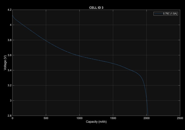
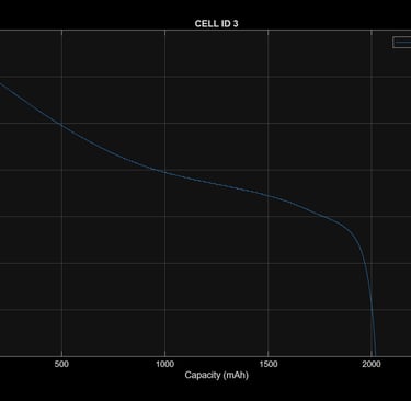
Full discharge curve of a Sony VTC4 cell generated using the cell data from V1.2 10-channel tester, ploted using MATLAB. The system maintained a stable 1.5A constant current discharge, yielding a capacity measurement that matched the manufacturer's datasheet within 5% and a DCIR of 33mohm. This data confirms the precision of the op-amp control loop over a full discharge cycle and MOSFET maintained a approximate 45-50C temperature.
Key Features:
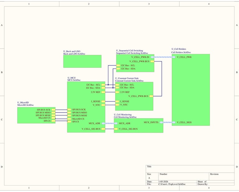
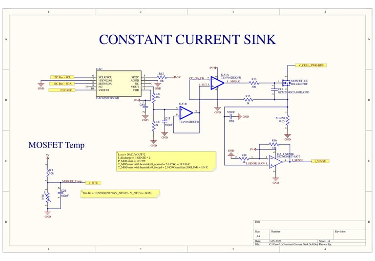
Precision Current Sink
The analog front-end features an IRLZ44N MOSFET, a TLV9162 control op-amp, and a low-side 50 mΩ shunt. Discharge controlled by I2C DAC60501ZDGSR 12-bit DAC; I_sense signal amplified by MCP6001. Shared 2.5 V precision reference for ADC/DAC.
Switching & MUX
Hardware-controlled sequential switching guarantees mutually exclusive channels via PCF8575PWR I2C expander and CD4514BM96 line decoder. Cell voltage is sampled by CD74HC4067SM96 16:1 analog MUX using quasi-Kelvin sensing.
Power Distribution
A 4-layer mixed-signal PCB (SIG/GND/PWR/SIG) integrates an AP64502QSP-13 synchronous buck converter for the 5V rail and a dedicated 3.3V LDO for MicroSD SPI.
Hardware Protection
Fault-tolerant protection includes MCQ7328-TP P-channel MOSFETs for reverse polarity, heatsink NTC for active over-temperature protection, and external relay flyback diodes
Calibration
I measured cell voltage readings and voltage drop across the shunt for the entire 4.2V to 2.5V range using a multimeter and modified firmware accordingly. There was no drift in the calibration over the voltage range.
Challenges Faced
1. Managing Thermal Dissipation at High Currents
The MOSFET has to dissipate all the current passing through as heat, so in the max case (5A), power dissipation is 19.75W. A heatsink and a fan would be needed.
Solution: Calculated the maximum allowable heat sink thermal resistance to be 4.33°C/W and used a heat sink with a thermal resistance of 2.6°C/W, providing a healthy margin. NTC on Load MOSFET's heatsink for active over-temperature protection.
2. Ensuring Analog Precision in a Noisy Environment
The analog front-end has to measure delicate cell voltage and current, so in the presence of 5A relay drive and switching currents, electrical noise interferes with the readings. Physical separation and low-impedance return paths would be needed.
Solution: A custom 4-layer mixed-signal PCB (SIG / GND / PWR / SIG) optimized for high-current power handling, precision analog measurement, and noise handling. GND and PWR planes are continuous and unbroken, providing low-impedance return paths and a stable reference plane. The quasi-Kelvin sense (separate PWR and SIG traces but shared GND) is used for current and voltage measurement.
3. Guaranteeing Mutually Exclusive Channels
The switching circuit has to connect high-energy 18650 cells to the discharge bus, so in the case of a software fault, connecting multiple channels simultaneously causes a short circuit. A hardware interlock would be needed.
Solution: A CD4514BM96 decoder to prevent connecting more than one channel at the same time and an active-high inhibit pin controlled by an I2C expander.
4. Interfacing Mixed Logic Levels
The 5V MCU has to write data to the 3.3V MicroSD and control the I²C expander. Voltage level translators would be needed.
Solution: A TXU0304PWR unidirectional voltage level translator for 5V to 3.3V for SCK, MOSI, and CS (MCU to MicroSD) and 3.3V to 5V for MISO (MicroSD to MCU). External pull-ups on all I2C lines.
5. Protecting Sensitive ICs from Reverse Polarity
The MUX has to sample cell voltage, so in the case of reverse polarity, the MUX's internal ESD clamp diode forward biases. Current limiting resistors would be needed to protect the MUX.
Solution: Reverse polarity protection for each channel using MCQ7328-TP P-channel MOSFETs, which protects everything except MUX. A current-limiting resistor (limits to 2.1 mA) on each channel to protect the MUX in case of reverse polarity, as cell voltage traces are connected straight to the cell holder for proper Kelvin sensing.
6. Manual Bring-Up and Debugging
Reduce manufacturing and assembly costs as much as possible due to budget constraints. Contingencies and Test points in case of design errors
Solution: Passive components are assembled by a fabrication house, and all of them have been placed on top for one-sided assembly. All ICs, cell holders, and connectors are hand-assembled post-fabrication to reduce assembly cost.
Discovered a reversed footprint on the MUX and improvised a solution by manually soldering a 28-pin SSOP breakout board directly to the PCB pads using a single copper strand extracted from 24 AWG wire.